| Appl. No. | US Patent Title |
|---|---|
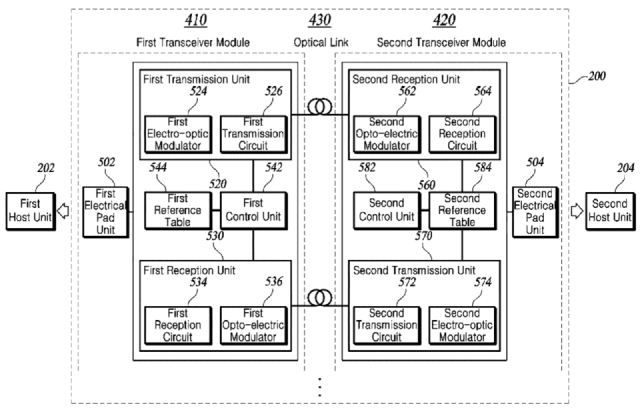
| 16/330,396 | Optical assembly for optical transceiver and optical transceiver using same |
| 16/887,097 | Fanout optical assembly |
| 16/849,218 | Active optical cable |
| 16/710,562 | Optical module |
| 16/429,351 | Active optical cable |
| 16/288,759 | Active optical cable |
| 15/956,987 | Optical assembly for light transmission and reception |
| 16/285,841 | Optical receiving device including focusing lens and reflector mounted to housing body and collimating lens mounted to housing cover |
| 16/008,774 | Optical receiving device including focusing lens and reflector mounted to housing body and collimating lens mounted to housing cover |
| 15/039,477 | Optical transceiver device |
| 14/750,211 | Method and apparatus for aligning optical element |
Key patents are registered in the following countries to protect our technology and product worldwide.
- US: 11, Korea: 12, Japan: 5, China: 3, EU: 1
US 11,012,158 B2
Active optical cable US 11,012,158 B2, May 18, 2021
Abstract
An active optical cable is disclosed.
According to the present disclosure, there is provided an active optical cable,
having no complicated structure by obviating the need for a separate monitoring photodetector as was used
for a typical optical transceiver, increasing light output-current linearity to improve optical coupling efficiency,
generating a library of transmission/reception-related electro-optical characteristics of both optical modules
so as to enable light outputted from a light source included in an optical transmitter to maintain high linearity
over a wide range of temperatures, thereby reducing power consumption, and being applicable to a multi-level
PAM technique involving at least four (4) levels.
US 10,268,007 B2
Optical transmitting device including first lens and reflector mounted to housing body and second lens mounted to housing cover US 10,268,007 B2, Apr. 23, 2019
Abstract
Embodiments according to the present disclosure relate to an optical transmitting device and an optical receiving device which can minimize the alignment error between the light source and the photodetector on the substrate, miniaturize the devices, and require no separate guide member reducing manufacturing costs, while satisfying the design requirements for sub-miniaturization, and performing optical transmission and reception more efficiently.
US 9,423,569 B2
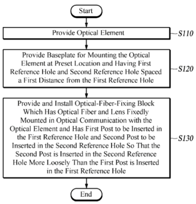
Method and apparatus for aligning optical element US 9,423,569 B2, Aug. 23, 2016
Abstract
A structure of aligning an optical element includes a baseplate including a set position for mounting at least one
optical element, a first reference hole, and a second reference hole spaced by a first distance from the first
reference hole.
The set position is determined by a first baseline that passes the first reference hole and
the second reference hole and a second baseline that intersects with the first baseline at a second distance
from the first reference hole on an opposite side to the second reference hole with respect to the first
reference hole.
The second distance is shorter than the first distance.